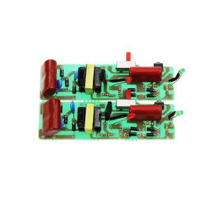
PCB has single-sided, double-sided and multi-layer. For radio and other simple appliances, single-sided PCB can be used. However, with the progress of the times, electronic products need to be updated, regardless of function or volume. For multi-functional, small volume electronic products, single-sided and double-sided PCB can not fully meet the requirements, but must use multi-layer PCB.
Multilayer PCB has many advantages, such as: high assembly density, small size; short connection between electronic components, fast signal transmission speed, convenient wiring; good shielding effect, and so on. At present, there are more than 100 layers of PCB, the common ones are four layers and six layers.
In the design of multilayer board, each layer should be symmetrical, and even copper layer is preferred. If it is asymmetric, it is easy to cause distortion. Multilayer board wiring is carried out according to the circuit function. When wiring in the outer layer, more wiring is required on the welding surface and less wiring is required on the component surface, which is conducive to the maintenance and troubleshooting of PCB. In terms of routing, it is necessary to separate the power supply layer, formation and signal layer to reduce the interference among power supply, ground and signal. The lines of the adjacent two layers of printed boards shall be perpendicular to each other or inclined lines and curves shall not be parallel lines, so as to reduce the interlayer coupling and interference of the base plate.
Compared with single-sided PCB and double-sided PCB, which layers are composed of? What does each layer represent and what is its use? Multilayer PCB mainly consists of the following layers: signal layer, internal planes, mechanical layers, masks, silk screen and system working layer.
The signal layer is divided into top layer, middle layer and bottom layer. It is mainly used to place various components, or for wiring and welding. The internal power layer is also called the internal power layer, which is specially used for arranging power lines and ground wires. The mechanical layer is generally used to place indicative information about the board making and assembly methods, such as physical dimension line, data data, via information, etc. The solder mask layer also has a top layer and a bottom layer. The pads or other objects placed on the layer are copper free areas. The screen printing layer is mainly used to draw the outline of the component, place the number of the component or other text information. The system working layer is used to display the information that violates the design rules.
Sep 28, 2019