PCB production process is more complex, it involves a wide range of processes, from simple machining to complex machining, there are common chemical reactions, photochemistry, electrochemistry, thermochemistry and other processes, CAD CAM and other knowledge. In addition, there are many process problems in the production process and new problems will be encountered from time to time. Some problems will disappear without finding out the causes. Because the production process is a kind of non continuous assembly line, any problem in any link will cause the whole line to stop production or a large number of waste reports. If the printed circuit board is scrapped, it cannot be recycled. The process engineer's work Because of the great pressure, many engineers left the industry and transferred to PCB equipment or material suppliers for sales and technical services.
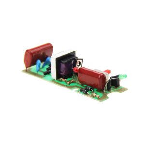
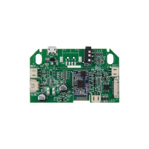
The base plate of the board itself is made of insulating and non bendable materials. The small circuit material that can be seen on the surface is copper foil. Originally, the copper foil is covered on the whole board. During the manufacturing process, some parts are etched away, and the remaining parts become network small circuits. These circuits are called conductor patterns or wiring, and are used for Provide circuit connection of parts on PCB.
In order to fix the parts on the PCB, we weld their pins directly on the wiring. On the most basic PCB (single panel), the parts are concentrated on one side, and the wires are concentrated on the other side. In this way, we need to drill holes in the board, so that the pins can pass through the board to the other side, so the pins of the parts are welded on the other side. Because of this, the PCB is positive and negative Faces are called component side and weld side, respectively.
If there are some parts on the top of PCB that can be removed or installed after the completion of manufacturing, socket will be used when the parts are installed. Because the socket is directly welded on the board, the parts can be disassembled and assembled at will.
If we want to connect two PCBs with each other, we usually use the edge connector commonly known as "golden finger". The golden finger contains many bare copper pads, which are actually part of PCB wiring. Usually, when connecting, we insert the golden finger on one PCB into the appropriate slot on the other PCB (commonly known as expansion slot). In the computer, like It is a display card, sound card or other similar interface card, which is connected to the main board by means of gold fingers.

The green or brown color on the PCB is the color of solder mask. This layer is an insulating protective layer, which can protect the copper wire and prevent the parts from being welded to the wrong place. In addition, a layer of silk screen will be printed on the solder mask. Generally, words and symbols (mostly white) will be printed on it to mark the position of each part on the board The printed surface is also called the legend.
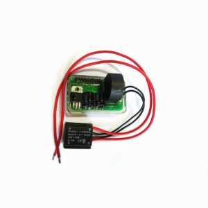
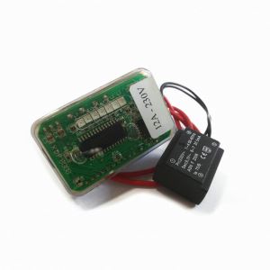
Printed circuit board etches the complex circuit copper wire between parts on a board after careful and neat planning, providing the main support body for the installation and interconnection of electronic components, which is an indispensable basic part of all electronic products.
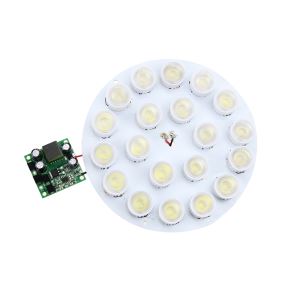
Printed circuit board is a flat plate made of non-conductive materials, on which there are usually pre drilled holes designed to install chips and other electronic components. The holes of the components help to connect the predefined metal paths printed on the board in an electronic way, pass the pins of the electronic components through the PCB, and then adhere the conductive metal electrodes on the PCB to form a circuit.
Nov 05, 2019