1. There should be a reasonable trend
Such as input / output, AC / DC, strong / weak signal, high frequency / low frequency, high voltage / low voltage, etc. Their trend should be linear (or separate) and should not blend with each other. Its purpose is to prevent mutual interference. The best trend is straight line, but it is not easy to achieve. The most unfavorable trend is circular. Fortunately, isolation can be set to improve. For DC, small signal, low voltage PCB design requirements can be lower. So "reasonable" is relative.
2. Choose a good grounding point: grounding point is often the most important
I don't know how many engineers and technicians have discussed the small grounding point, which shows its importance. In general, common ground is required, such as: multiple ground wires of forward amplifier shall be connected with the main ground after merging. In reality, it is difficult to do it completely because of various restrictions, but we should try our best to follow it. This problem is quite flexible in practice. Everyone has his own set of solutions. It is easy to understand if it can be explained according to the specific circuit board.
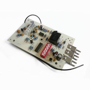
3. Reasonably arrange power filter / decoupling capacitor
Generally, only a few power filter / decoupling capacitors are drawn in the schematic diagram, but where they should be connected is not indicated. In fact, these capacitors are set for switching devices (gate circuits) or other components that need filtering / decoupling. The arrangement of these capacitors should be as close to these components as possible, and they will not work if they are too far away. Interestingly, when the arrangement of power filter / decoupling capacitor is reasonable, the problem of grounding point is not so obvious.
4. The line diameter requires that the through-hole size of the buried hole is appropriate
If conditions permit, the wide line shall never be thin; the high-voltage and high-frequency lines shall be smooth, without sharp chamfering, and the right angle shall not be used for turning. The ground wire should be as wide as possible, and it is better to use large area of copper laying, which greatly improves the problem of butt joint location. The size of pad or wire hole is too small, or the pad size does not match the drilling size properly. The former is disadvantageous to manual drilling and the latter to numerical control drilling. It is easy to drill the pad into a "C" shape, and if it is heavy, the pad will be drilled out. The conductor is too thin, and the large area of non wiring area is not set with copper coating, which is easy to cause uneven corrosion. That is to say, when the non wiring area is corroded, the fine wire is likely to be corroded excessively, or it seems to be broken, or completely broken. Therefore, setting copper is not only to increase the area of ground wire and anti-interference.
5. Number of vias, solder joints and linear density
Some problems are not easy to be found in the early stage of circuit manufacturing, they often emerge in the later stage, such as too many wire holes, copper deposition process will bury hidden dangers if there is a little carelessness. Therefore, the design should minimize the line hole. The density of parallel lines in the same direction is too large, so it is easy to connect them when welding. Therefore, the linear density should be determined according to the level of welding process. The distance between welding points is too small, which is not conducive to manual welding, so the welding quality can only be solved by reducing the work efficiency. Otherwise, there will be hidden danger. Therefore, the determination of the minimum distance of the welding spot should consider the quality and work efficiency of the welding personnel.
If we can fully understand and master the above PCB design considerations, we can greatly improve the design efficiency and product quality. Correcting the mistakes in the production will save a lot of time and cost, and save rework time and material input.
ive key points of PCB design!
Sep 01, 2019